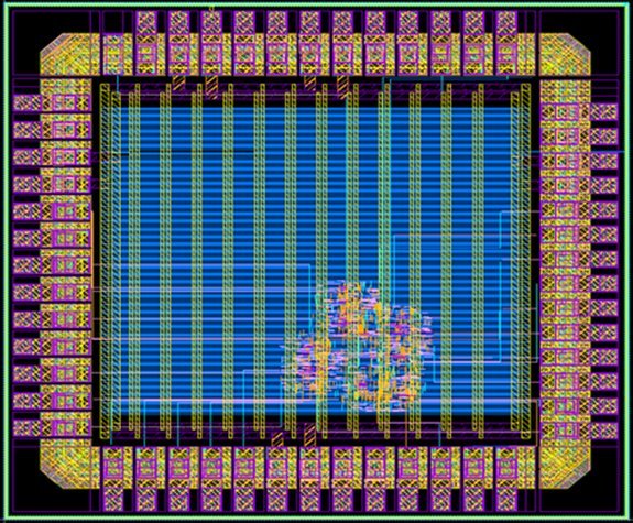
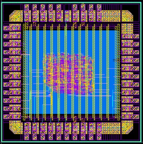
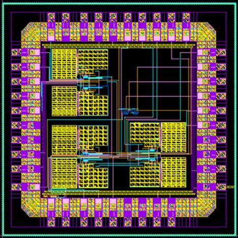
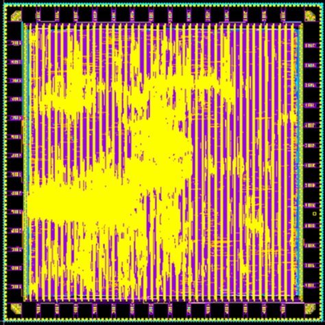
End-to-end semiconductor design services — SoC Engineering, FPGA-based SoC, Embedded Systems, High Speed Design, and AI Accelerators. Trusted globally.
Angstromers Engineering Solutions is a premier semiconductor design services company delivering end-to-end engineering solutions. We specialize in deep silicon design and work across the complete product lifecycle — from specification through tapeout and beyond.
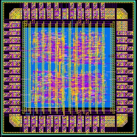
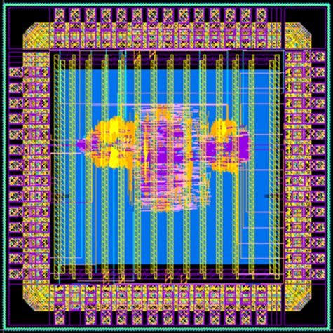
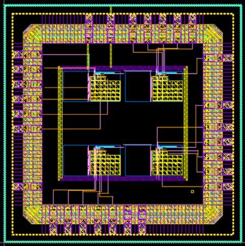
With a focused team of 25+ seasoned engineers and a track record of 75+ projects and 18+ real chip tapeouts delivered globally, we've built a reputation for technical depth, schedule adherence, and quality of execution.
ASIC Front-end Microarchitecture Design & Implementation, ASIC/SoC Verification Signoff and RTL to GDS tasks, including customized AMS chip design.
SoC-FPGA based design integration, implementation & testing on target board including firmware development for built-in CPU cores and ASIC prototyping.
Core embedded systems development from device driver layer to application layer with expertise implementing software on Multi-Core CPU architectures.
Board design, signal integrity analysis, re-engineering, developing high-speed interconnect solutions and Data Acquisition Systems for demanding applications.
DNN Accelerator Development & Deployment, Compiler Toolchain for AI-DNN processors, and custom hardware accelerator design for ML workloads.
Complete turnkey solutions covering IC packaging, design and production of interconnect materials, front-end engineering test, wafer probing and final test.
Real chip layouts — from RISC-V processors and DSP cores to PLLs, ADCs, DACs, and LNAs — taped out on Skywater 130nm and advanced FinFET nodes.
Deep-dive technical projects spanning SoC engineering, FPGA verification, embedded systems, and accelerator deployments.
Custom layout of blocks 12nm FinFET — Physical Verification (DRC, LVS) and LPE extraction. Tight MPW schedule met.
Development from Specifications to GDS-II including custom circuit and layout design. Characteristic verification, optimized power/area.
Full RISC-V compatible processor tapeout on Skywater 130nm. From RTL to GDS-II with full DRC/LVS sign-off and characteristic verification.
Custom LNA design and tapeout — RF front-end analog block for signal chain applications. Post-layout simulation completed.
High-performance FFT coprocessor with RISC-V compatibility on Skywater 130nm. AXI stream architecture for seamless SoC integration.
Flexible reconfigurable ADC architecture on Skywater 130nm. SAR and VDA topologies with analog PLL integration for clock generation.
A culture of empowerment, learning, and growth — hear from the engineers who build with us.
I feel empowered with the kind of experiences I've had here. The mentorship and real-world exposure to complex SoC projects from day one is incredible.
A very good company to start your career. Colleagues are approachable, supportive, and helpful. Lots of opportunities for professional and personal growth in VLSI.
The right platform to kickstart your career in the VLSI domain. The ecosystem keeps us learning continuously with excellent challenges and strong recognition of performance.
We're always looking for talented engineers across SoC, FPGA, embedded, and accelerator domains. Open roles for all experience levels.
Apply NowOpen culture with approachable leadership. Real-world SoC and FPGA project exposure, real chip tapeout experience, continuous technical growth, and a collaborative environment — while delivering world-class semiconductor engineering.
Ready to start a project or explore a partnership? Our engineering team is ready to discuss your requirements and deliver world-class semiconductor solutions.